This study material has been compiled and organized from a provided copy-pasted text and a lecture audio transcript.
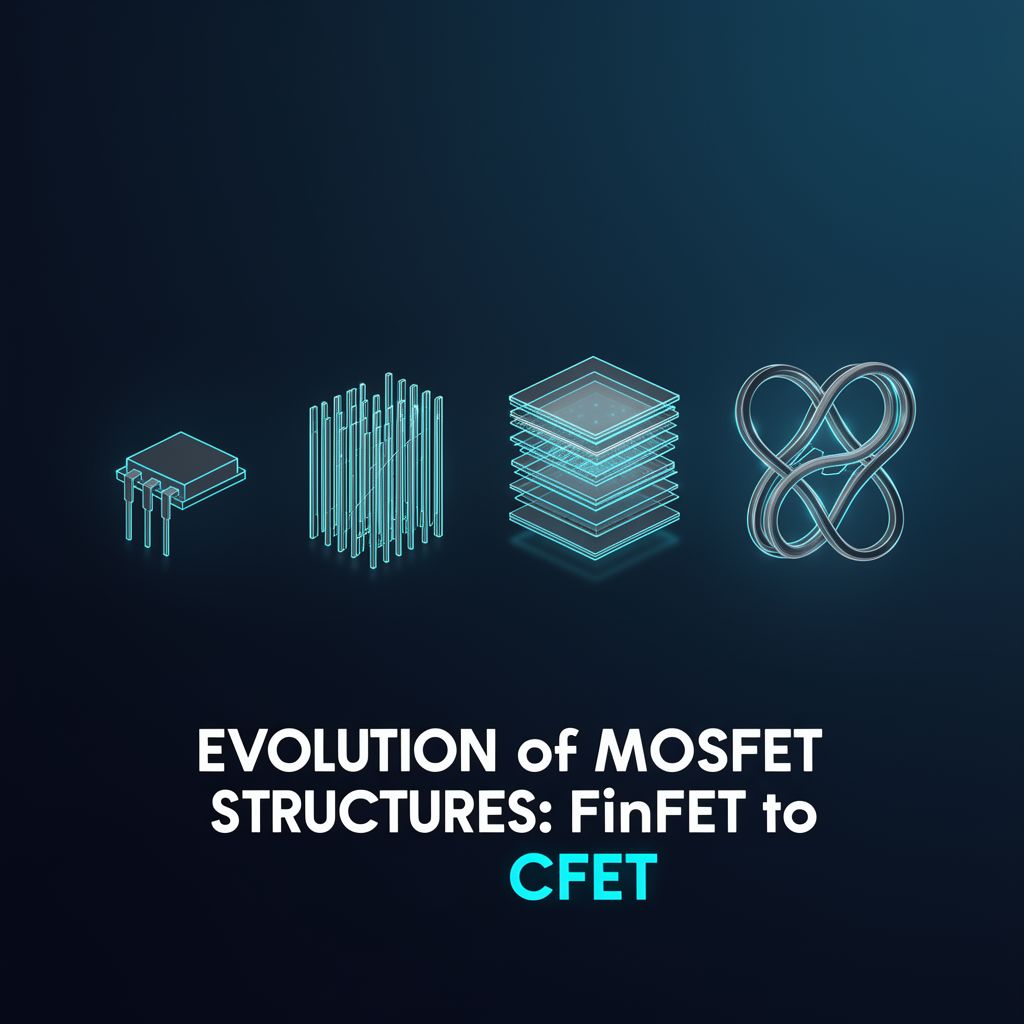
📚 MOSFET Miniaturization: Challenges, Scaling, and Device Evolution
📝 Introduction to MOSFET Scaling
The continuous miniaturization of Metal-Oxide-Semiconductor Field-Effect Transistors (MOSFETs) has been a primary driving force in the semiconductor industry, leading to significant advancements in device and circuit performance. Reducing the channel length (L) offers numerous benefits:
- Improved Performance ✅:
- Faster Frequency Response: A quadratic decrease in transit time ($t_{tr}$) with reduced L allows for faster analog circuits.
- Increased Current Availability: Drain current ($I_{DS}$) increases due to inverse proportionality with L.
- Faster Logic Circuits: Intrinsic capacitances ($C_{GS}$, $C_{GD}$) decrease linearly with L, leading to faster switching speeds.
- Higher Integration Density ✅: Smaller transistors occupy less area on the silicon wafer, allowing more devices to be integrated, which reduces cost per device and drives technological evolution.
- Cost Reduction ✅: Increased integration density with cost-effective processes lowers the manufacturing cost per device or per logic function.
However, these benefits are only realized when the reduction of L is moderate. When L is drastically reduced without corresponding changes to other device parameters, the transistor enters the "short-channel regime", leading to a significant worsening of performance and operation. This regime introduces new, unexpected dependencies on physical parameters, necessitating a fundamental shift in design and modeling approaches.
⚠️ The Short-Channel Regime: Onset and Detrimental Effects
The short-channel regime arises when physical effects, previously negligible in long-channel analysis, become dominant due to reduced L. These effects negatively impact transistor performance and reliability.
1️⃣ Bidimensional Electrostatics in the Channel
In long-channel MOSFETs, the gradual-channel approximation simplifies electrostatics to a quasi-one-dimensional problem. Source and drain regions primarily set boundary conditions. However, in short-channel devices, the influence of source and drain regions extends significantly into the channel, making electrostatics strongly two-dimensional (2D).
-
Visualizing Electrostatics 📊:
- Figure 27 (a) & (b): Long-Channel MOSFET EC Profile
- Description: Shows the schematic structure and the Conduction Band Edge ($E_C$) profile along the y-direction (channel length) at the semiconductor surface for a long-channel MOSFET with $V_{DS}=0$ and $V_{FB} < V_{GS} < V_T$.
- Explanation: Over most of the channel, $E_C$ is relatively flat and far from the Fermi level ($E_F$), indicating quasi-1D electrostatics. Only at the very edges, near the source and drain, does $E_C$ bend strongly to approach $E_F$ due to the high $n^+$ doping. This bending is a small fraction of L and thus negligible.
- Figure 27 (c) & (d): Short-Channel MOSFET EC Profile
- Description: Shows the schematic structure and $E_C$ profile for a short-channel MOSFET under the same conditions.
- Explanation: When L is reduced, the transition regions where $E_C$ bends from the source/drain edges become a significant fraction of L and can even merge. This creates a "bell-shaped" $E_C$ profile centered in the channel, with no flat-band region. This visual change signifies that channel electrostatics are now strongly 2D, rendering the gradual-channel approximation inaccurate.
- Figure 27 (a) & (b): Long-Channel MOSFET EC Profile
-
Consequences of Bidimensional Electrostatics:
-
a) Short-Channel Effect (VT Roll-off) 📉:
- Definition: A decrease in the threshold voltage ($V_T$) as L is reduced.
- Mechanism: The bell-shaped $E_C$ profile in short-channel devices means the peak $E_C$ is lower than in a long-channel device for the same $V_{GS}$. This effectively increases the electron concentration in the channel, meaning a lower $V_{GS}$ is required to achieve strong inversion.
- Figure 28: VT Trend with L
- Description: Plots the change in $V_T$ ($\Delta V_T$) relative to the long-channel value as L decreases. It also shows the impact of different $V_{DS}$ values.
- Explanation: For long L, $V_T$ is almost independent of L. As L decreases and the device enters the short-channel regime, $V_T$ rapidly drops (rolls off). This drop is more pronounced for higher $V_{DS}$, indicating a dependence of $V_T$ on $V_{DS}$ in the short-channel regime.
-
b) Drain-Induced Barrier Lowering (DIBL) 💡:
- Definition: A decrease in $V_T$ with an increase in $V_{DS}$, particularly for short L.
- Mechanism: In short-channel devices, the drain $n^+$ region's influence on channel electrostatics is significant. An increase in $V_{DS}$ pulls the entire $E_C$ profile downwards, lowering the peak of the $E_C$ barrier. This effectively increases the electron concentration for a given $V_{GS}$, allowing strong inversion at a lower $V_{GS}$ (i.e., lower $V_T$).
- Figure 29: Impact of VDS on EC Profile
- Description: Compares the effect of increasing $V_{DS}$ on the $E_C$ profile for (a) long-channel and (b) short-channel MOSFETs.
- Explanation: In a long-channel device (a), increasing $V_{DS}$ only causes a stronger $E_C$ drop near the drain, with the central channel region largely unaffected. In a short-channel device (b), the entire $E_C$ profile is dragged downwards, and the peak $E_C$ is lowered and shifted leftwards, directly illustrating DIBL.
-
c) Increased OFF-State Current ($I_{OFF}$) and Subthreshold Swing (STS) Degradation 📈:
- Impact: $V_T$ dependencies on L and $V_{DS}$ complicate circuit design, worsen $V_T$ variability, and degrade output resistance. Most critically, they lead to an exponential increase in $I_{OFF}$ and static power dissipation.
- Figure 30: $I_{DS}-V_{GS}$ Transcharacteristics
- Description: Compares $I_{DS}-V_{GS}$ curves for (a) long-channel and (b) short-channel MOSFETs at different $V_{DS}$ values.
- Explanation: For a long-channel device (a), $V_{DS}$ primarily affects $I_{DS}$ in the ON-state. For a short-channel device (b), increasing $V_{DS}$ causes an exponential growth of $I_{DS}$ in the subthreshold regime (i.e., $I_{OFF}$ increases significantly). This is a direct result of $V_T$ reduction with $V_{DS}$ (DIBL).
- Punch-Through: For very short L or high $V_{DS}$, the gate loses control over channel electrostatics, leading to a condition called "punch-through." The energy barrier blocking electron flow from source to drain is severely reduced or removed, resulting in a persistently high $I_{DS}$ even in the OFF-state (e.g., magenta curve in Fig. 30(b)).
-
-
Quantitative Analysis of Bidimensional Electrostatics:
- The shift in $V_T$ ($\Delta V_T$) due to short-channel effects can be approximated by:
$|\Delta V_T| = \frac{24t_{ox}}{W_d^{max}} \phi_{bi}(\phi_{bi} + V_{DS}) - 0.4 \cdot 2|\phi_B| e^{-\pi L / (2(W_d^{max} + 3t_{ox}))}$ (Eq. 67)
- This formula shows exponential dependence on L and square-root dependence on $V_{DS}$.
- Characteristic Length (L): To limit the impact of bidimensional electrostatics, a design constraint is introduced:
$L > 2(W_d^{max} + 3t_{ox})$ (Eq. 68)
- This defines a characteristic length $L_c = 2(W_d^{max} + 3t_{ox})$. If $L \gg L_c$, the device is long-channel. If $L < L_c$, it's a poor short-channel device.
- Design Implications: There is no absolute L value for short-channel behavior; it depends on $t_{ox}$ and $W_d^{max}$. Reducing L must be accompanied by reducing $t_{ox}$ (improves gate control) and $W_d^{max}$ (by increasing $N_a$, making $E_C$ transitions steeper).
- The shift in $V_T$ ($\Delta V_T$) due to short-channel effects can be approximated by:
$|\Delta V_T| = \frac{24t_{ox}}{W_d^{max}} \phi_{bi}(\phi_{bi} + V_{DS}) - 0.4 \cdot 2|\phi_B| e^{-\pi L / (2(W_d^{max} + 3t_{ox}))}$ (Eq. 67)
2️⃣ Velocity Saturation in the Channel
In long-channel MOSFETs, electron drift velocity ($v_d$) is assumed proportional to the electric field ($F_y$). However, in short-channel devices, $F_y$ can become very high, causing $v_d$ to reach a maximum saturation velocity ($v_{sat}$).
-
Drift Velocity vs. Electric Field 📈:
- Figure 31: Drift Velocity Trend with Fy
- Description: Shows the typical trend of drift velocity ($v_d$) versus electric field ($F_y$) on a log-log scale for electrons and holes.
- Explanation: At low $F_y$, $v_d$ is proportional to $F_y$ ($v_d \propto \mu_{eff} F_y$). As $F_y$ increases, $v_d$ eventually saturates at $v_{sat}$. This non-linear relationship is crucial for short-channel devices.
- Phenomenological Relation:
$v_d = \frac{\mu_{eff} \cdot |F_y|}{(1 + (|F_y|/F_{sat})^{\tilde{n}})^{1/\tilde{n}}}$ (Eq. 69)
- Where $F_{sat}$ is the field at which saturation occurs, $\mu_{eff}$ is the effective low-field mobility, and $\tilde{n}$ is a constant (2 for electrons, 1 for holes).
- Figure 31: Drift Velocity Trend with Fy
-
Impact on $I_{DS}$ and Saturation:
- Velocity saturation reduces the current availability and causes earlier saturation of the $I_{DS}-V_{DS}$ curve.
- Generalized $I_{DS}$ Formula:
$I_{DS} = \frac{\mu_{eff} C_{ox} \frac{W}{L} ((V_{GS}-V_T) V_{DS} - m \frac{V_{DS}^2}{2})}{1 + \frac{1}{F_{sat}} \frac{V_{DS}}{L}}$ (Eq. 70)
- This formula shows that for short L, the denominator increases, reducing $I_{DS}$ compared to the long-channel prediction.
- Figure 32: $I_{DS}-V_{DS}$ Characteristic with Velocity Saturation
- Description: Compares the $I_{DS}-V_{DS}$ curve for a short-channel MOSFET with and without accounting for velocity saturation.
- Explanation: The "Actual device characteristic" (red curve, with velocity saturation) shows an earlier and lower saturation of $I_{DS}$ compared to the "Long-channel analysis" (blue curve, neglecting velocity saturation). This demonstrates the reduction in current availability and earlier saturation due to velocity saturation.
- Saturated Drain Voltage ($V_{DS}^{sat}$): In the presence of velocity saturation, $V_{DS}^{sat}$ is lower than predicted by long-channel analysis. $V_{DS}^{sat} = \frac{2(V_{GS}-V_T)/m}{1 + \sqrt{1 + \frac{2(V_{GS}-V_T)}{F_{sat}mL}}}$ (Eq. 71)
- Saturated Drain Current ($I_{DS}^{sat}$): Velocity saturation changes the dependence of $I_{DS}^{sat}$ on $V_{GS}-V_T$.
- Figure 33: $I_{DS}^{sat}$ vs. Gate Overdrive
- Description: Plots $I_{DS}^{sat}$ against $V_{GS}-V_T$ for different L values, comparing results from Eq. 72 (with velocity saturation) and Eq. 26 (long-channel).
- Explanation: For long L, both formulas yield similar quadratic dependence. For short L, $I_{DS}^{sat}$ is significantly lower when velocity saturation is accounted for, and its dependence on $V_{GS}-V_T$ shifts from quadratic towards linear as L decreases.
- Figure 33: $I_{DS}^{sat}$ vs. Gate Overdrive
- Mechanism of Saturation: When velocity saturation is relevant, $I_{DS}$ saturates not because the inversion charge vanishes (pinch-off), but because electrons reach $v_{sat}$ at the drain side of the channel.
$I_{DS}^{sat} = -W Q_{inv}(y=L, V_{DS}=V_{DS}^{sat}) v_{sat}$ (Eq. 73)
- In the limit of $L \to 0$, $v_d$ reaches $v_{sat}$ everywhere, leading to a linear dependence: $I_{DS}^{sat} = W C_{ox} (V_{GS}-V_T) v_{sat}$ (Eq. 74)
-
Hot Electron Effects ⚠️:
- Mechanism: In short channels, high electric fields (especially near the drain) can accelerate electrons to very high kinetic energies between scattering events. These are called "lucky electrons" or "hot electrons."
- Figure 34: Schematic Band Diagram for Hot Electrons
- Description: Shows a band diagram in the y-direction highlighting how hot electrons can reach very high energy levels in the conduction band.
- Explanation: The strong band bending allows some electrons to gain significant energy, overcoming the energy barrier of the insulator.
- Reliability Issues: Hot electrons can cause:
- Gate leakage currents by overcoming the insulator barrier.
- Impact ionization in the channel.
- Creation of interface states by breaking bonds at the semiconductor surface.
- Challenge: Controlling $F_y$ to prevent hot electron generation is crucial for device reliability.
📈 MOSFET Scaling Rules
To mitigate the detrimental effects of short-channel phenomena, MOSFET miniaturization must follow specific scaling rules that adjust all device parameters.
1️⃣ Constant-Field Scaling Rules (Dennard Scaling, 1974)
- Goal: Miniaturize MOSFETs while keeping electric fields within the device constant.
- Principles 📚:
- Figure 35: Schematic of MOSFET Miniaturization
- Description: Illustrates how dimensions are reduced from an (a) original device to a (b) miniaturized device.
- Explanation: All horizontal and vertical dimensions are scaled down by a factor $k > 1$.
- Scaling Parameters (Table 1):
- Dimensions (L, W, $t_{ox}$, $X_j$, etc.): $1/k$
- Voltages ($V_{GS}$, $V_{DS}$, $V_{BS}$): $1/k$
- Doping Concentrations ($N_a$, $N_d$): $k$ (derived from Poisson's equation to maintain constant electric fields)
- Figure 35: Schematic of MOSFET Miniaturization
- Impact on Device & Circuit Parameters (Table 2):
- Positive:
- Electric fields & drift velocity: 1 (constant)
- Capacitances: $1/k$
- Carrier transit time: $1/k$ (leading to faster circuits)
- Delay time of logic gates: $1/k$
- Power dissipation (per device): $1/k^2$
- Density of power dissipation (per unit area): 1 (constant, good for heat management)
- Integration density: $k^2$ (major benefit)
- Limitations ⚠️:
- Unscalable $V_T$: $V_T$ cannot be perfectly scaled by $1/k$ because $2|\phi_B|$ (related to the energy gap) is a fundamental material property and cannot be freely changed. This necessitates structural changes (e.g., non-uniform substrate doping).
- Increased $I_{OFF}$: The subthreshold swing (STS) is proportional to $kT/q$, which cannot be scaled.
- Figure 36: Impact on $I_{OFF}$
- Description: Pictorial view showing the $I_{DS}-V_{GS}$ curve for an original and a scaled device.
- Explanation: The reduction of $V_T$ without a corresponding reduction in STS leads to an exponential increase in $I_{OFF}$ for the scaled device. This increases static power dissipation.
- Figure 36: Impact on $I_{OFF}$
- Incomplete Avoidance of Short-Channel Effects: $W_d^{max}$ decreases by less than $k$, meaning the miniaturized device is still more susceptible to bidimensional electrostatics than the original.
- Compatibility Issues: Requires changing operating voltages for each new generation, leading to system-level incompatibility.
- Positive:
2️⃣ Generalized Scaling Rules (Baccarani Scaling, 1984)
-
Goal: Tolerate a controlled increase in electric fields to mitigate drawbacks of constant-field scaling.
-
Principles 📚:
- Dimensions (L, W, $t_{ox}$, $X_j$, etc.): $1/k$
- Voltages ($V_{GS}$, $V_{DS}$, $V_{BS}$): $\alpha/k$ (where $1 \le \alpha \le k$, allowing electric fields to increase by $\alpha$)
- Doping Concentrations ($N_a$, $N_d$): $\alpha k$
- Special Cases:
- $\alpha = 1$: Reduces to constant-field scaling.
- $\alpha = k$: Becomes constant-voltage scaling (voltages remain unchanged).
-
Impact on Device & Circuit Parameters (Table 4):
- Benefits:
- Better immunity to bidimensional electrostatics (stronger reduction of $W_d^{max}$).
- Stronger improvements in device and circuit performance (e.g., carrier transit time decreases by $\alpha k$ or $k$, increasing cut-off frequency).
- Mitigates $I_{OFF}$ growth (can eliminate it with constant-voltage scaling).
- Allows for constant operating voltages (improving compatibility).
- Trade-offs ⚠️:
- Increased velocity saturation effects (electric fields increase by $\alpha$).
- Worsened device reliability (due to higher electric fields).
- Increased ON-state power dissipation per unit area (power dissipation density grows by $\alpha^3$ or $\alpha^2$), posing heat removal challenges.
- Benefits:
-
Historical Application: CMOS technology evolution has used a combination of constant-voltage and constant-field scaling steps to balance these trade-offs, leading to increasing relevance of bidimensional electrostatics, velocity saturation, and challenges in power dissipation and reliability.
🛠️ Evolution of MOSFET Device Structure
As scaling progresses, hard limits are encountered that necessitate fundamental changes to the MOSFET's structure, materials, or doping profiles.
1️⃣ The $t_{ox}$ vs. $W_d^{max}$ Design Space
Constraints on key parameters define an acceptable design space for $t_{ox}$ and $W_d^{max}$.
- Constraints:
- Subthreshold Swing (STS): Requires $m < 1.4$, leading to $t_{ox} < 0.13 W_d^{max}$ (Eq. 77).
- $\Delta V_T$ from Bidimensional Electrostatics: Requires $\Delta V_T < 100 \text{ mV}$, leading to $t_{ox} < L/6 - W_d^{max}/3$ (Eq. 78).
- Device Reliability (Gate Oxide Electric Field): Requires $F_{ox} < F_{ox}^{max}$, leading to $t_{ox} > V_{dd}/F_{ox}^{max}$ (Eq. 79).
- Figure 37: $t_{ox}$ vs. $W_d^{max}$ Design Space
- Description: A plot showing the three constraints (Eq. 77, 78, 79) in the $t_{ox}$ vs. $W_d^{max}$ plane. The green triangular region represents the acceptable design space.
- Explanation: This graph visually demonstrates that proper transistor design requires satisfying all three constraints simultaneously. The upper vertex of the green area indicates $t_{ox}^{max} \approx L/20$, highlighting that reducing L necessitates a reduction in $t_{ox}$. The lower boundary from reliability (Eq. 79) implies that $V_{dd}$ must also decrease with L to maintain design margins.
2️⃣ Gate Leakage and the High-k/Metal-Gate Stack
A critical hard limit emerged from gate leakage current as $t_{ox}$ was aggressively reduced.
-
Problem with Thin $\text{SiO}_2$:
- $\text{SiO}2$ is an excellent insulator, but as $t{ox}$ decreases, it becomes a worse barrier.
- Figure 38 (a): Gate Leakage Mechanisms
- Description: Schematic showing various physical mechanisms contributing to gate leakage: Direct Tunneling (DT), Trap-Assisted Tunneling (TAT), and Channel Hot-Electron (CHE) injection.
- Explanation: These mechanisms allow charge carriers to flow between the gate and the channel, even when the gate dielectric is nominally insulating.
- Quantum-Mechanical Tunneling: The most relevant mechanism for thin $\text{SiO}_2$.
- Figure 38 (b): Tunneling Gate Current vs. $F_{ox}$
- Description: Plots tunneling gate current density against oxide electric field ($F_{ox}$) for different $t_{ox}$ values. Insets show band diagrams for Fowler-Nordheim (FN) and Direct Tunneling (DT) regimes.
- Explanation: In the direct-tunneling regime (typical for modern $V_{dd}$), reducing $t_{ox}$ exponentially increases the gate leakage current, even if $F_{ox}$ is constant. This is because the tunneling barrier becomes thinner.
- Figure 38 (b): Tunneling Gate Current vs. $F_{ox}$
- Impact: Gate leakage is a spurious current and a significant source of static power dissipation. A maximum tolerable gate current density (e.g., $100 \text{ A/cm}^2$) sets a hard lower limit on $t_{ox}$ (e.g., $t_{ox} > 1.5 \text{ nm}$), which cannot be easily moved by reducing $V_{dd}$.
-
Solution: High-k Dielectrics 💡:
- When $t_{ox}^{max}$ (from STS and $\Delta V_T$ constraints) reached the minimum $t_{ox}$ set by gate leakage, a structural change was needed.
- Concept: Replace $\text{SiO}2$ with a material having a higher dielectric constant ($\epsilon{hk}$), called a "high-k" dielectric.
- Benefit: A physically thicker high-k layer ($t_{hk}$) can achieve the same electrostatic coupling (capacitance $C_{ox}$) as a much thinner $\text{SiO}2$ layer.
$C{ox} = \frac{\epsilon_{ox}}{t_{ox}} = \frac{\epsilon_{hk}}{t_{hk}} \implies t_{hk} = t_{ox} \frac{\epsilon_{hk}}{\epsilon_{ox}}$ (Eq. 80)
- The equivalent $\text{SiO}2$ thickness (EOT) is $t{ox} = t_{hk} \frac{\epsilon_{ox}}{\epsilon_{hk}}$.
- Figure 39: Schematic Band Diagram for High-k
- Description: Compares band diagrams for (a) an $\text{SiO}2$ layer of thickness $t{ox}$ and (b) a high-k layer of thickness $t_{hk}$ (where $t_{hk} > t_{ox}$) with the same EOT.
- Explanation: The thicker physical high-k layer (b) significantly reduces tunneling current compared to the thinner $\text{SiO}_2$ layer (a), even if the energy barrier height might be lower for high-k materials.
- Materials: Hafnium-based oxides (e.g., $\text{HfO}_2$, $\text{HfSiO}4$) with $\epsilon{hk}$ between 10 and 25.
- Challenges: High-k materials often have smaller energy gaps and more spurious states, affecting leakage and reliability (charge trapping). A very thin $\text{SiO}_2$ layer is often kept between the high-k and silicon to preserve interface quality.
-
Solution: Metal Gates 💡:
- Introduced alongside high-k dielectrics (first mass production in 2008).
- Reason: To eliminate parasitic voltage drops within the traditional highly-doped polysilicon gate, which became increasingly problematic with generalized scaling.
- Method: "Replacement gate" approach, where a sacrificial polysilicon gate is later replaced by metal, maintaining self-aligned processing.
🏁 Conclusion
MOSFET miniaturization has been a complex journey, driven by performance and cost benefits but constantly challenged by physical limits. The transition from long-channel to short-channel behavior introduces detrimental effects like bidimensional electrostatics (VT roll-off, DIBL, increased $I_{OFF}$) and velocity saturation (reduced current, hot electrons). Scaling rules (constant-field and generalized) provide guidelines for parameter adjustment, each with its own trade-offs. Ultimately, fundamental structural changes, such as the adoption of high-k dielectrics and metal gates, have been crucial in overcoming hard limits (like gate leakage) and extending the dominance of CMOS technology. This continuous evolution highlights the need for innovative device design to meet the demands of higher integration densities and improved performance.