This study material has been compiled from a copy-pasted text and an audio lecture transcript, providing a comprehensive overview of MOSFET evolution and miniaturization challenges.
📚 MOSFET Evolution and Miniaturization: From Planar to CFET
💡 Introduction: The Miniaturization Journey of Transistors
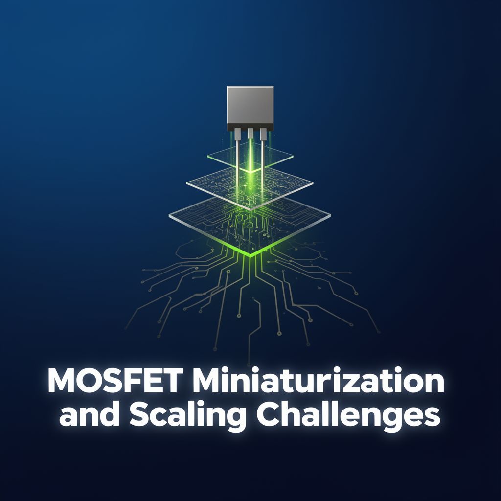
The continuous drive for increased integration density and improved performance in modern electronic devices has led to a remarkable evolution in MOSFET (Metal-Oxide-Semiconductor Field-Effect Transistor) structures. This study guide explores the challenges encountered during transistor miniaturization, the innovative structural solutions developed to overcome these hurdles, and the overarching influence of Moore's Law. We will delve into the transition from traditional planar MOSFETs to advanced architectures like FinFETs, Nano-sheet FETs (NSFETs), Forks-sheet FETs (FSFETs), and Complementary FETs (CFETs), detailing the reasons behind these transitions and their technological advantages. Each structural innovation represents a strategic response to specific physical limitations, pushing the boundaries of integrated circuit technology.
1️⃣ Gate-Last Process and Work Function Metals
In advanced CMOS manufacturing, a "gate-last" process is often employed, where the gate is formed after the source and drain regions. This approach is crucial for achieving proper calibration of the threshold voltage (VT) for both n-channel and p-channel transistors.
- VT Calibration: Different metals are used for the gates of n-channel and p-channel transistors to achieve precise VT calibration.
- Work Function Metal: A thin layer of metal, known as the "work function metal," is deposited on top of the high-k dielectric.
- Purpose: Its work function is carefully selected to establish the correct band alignment between the gate and the substrate under flat-band conditions.
- Examples: Common work function metals include TiN, TaN, TiAl, or other compounds based on these materials.
- Main Metal Deposition: After the work function metal, a main metal (e.g., Aluminum or Tungsten) is deposited to complete the gate stack and device integration.
2️⃣ Planar MOSFET Limitations and the Need for Structural Change
The miniaturization of traditional planar MOSFETs faced significant constraints, primarily related to the reduction of gate oxide thickness (tmax_ox) and supply voltage (Vdd). These reductions profoundly impacted off-state current (IOFF) and standby power dissipation.
2.1 📈 IOFF and Vdd Constraints
- Vdd Reduction and VT: To maintain a sufficient gate overdrive (Vdd - VT) for fast ON-state operation (e.g., in logic gates), a reduction in Vdd necessarily requires a corresponding reduction in VT. A common requirement is VT being one-fourth of Vdd.
- Impact on IOFF: However, decreasing VT exponentially increases IOFF. This is because the subthreshold slope (STS) of the transistor cannot be significantly improved in planar devices (typically around 85 mV/dec at room temperature for tmax_ox).
- Hard Constraint: A maximum acceptable IOFF (e.g., 100 nA/µm) sets a minimum VT (around 250 mV) and, consequently, a minimum Vdd (around 1 V). This is considered a "hard constraint" because there are no design parameters available to mitigate it.
2.2 ⚠️ Electric Field in Oxide and Trade-offs
- Electric Field vs. IOFF:
- To prevent excessive electric field in the oxide, Vdd must be reduced along with tmax_ox, but this increases IOFF.
- To prevent excessive IOFF, Vdd must remain constant, but this increases the electric field in the oxide.
- Vanishing Design Margins: This inherent trade-off between Vdd, IOFF, and the electric field in the oxide eventually eliminated design margins. When these hard constraints were reached, the only viable path for continued CMOS miniaturization was to fundamentally change the transistor's structure.
3️⃣ The Rise of FinFET Technology
The FinFET (Fin Field-Effect Transistor) emerged as a revolutionary structural change to overcome the limitations of planar MOSFETs, particularly concerning gate control over the channel without needing to further reduce tmax_ox.
3.1 📚 FinFET Structure and Operation
- Channel Geometry: The channel in a FinFET is a very thin, vertical pillar or "fin" of monocrystalline silicon, created on the wafer surface using photolithographic and etching steps.
- Gate Wrapping: The high-k/metal-gate stack covers the fin on three sides. This is why it's often called a "tri-gate transistor" or "three-dimensional (3D) transistor."
- Source and Drain: The source and drain regions are located at the longitudinal edges of the fin.
3.2 ✅ Advantages of FinFETs
- Enhanced Electrostatic Control: The gate's control over channel electrostatics is significantly better than in a planar MOSFET with the same tmax_ox. This is due to:
- Thin Fin: The fin's extremely small thickness (typically below 10 nm).
- Gate Wrapping: The gate's ability to wrap around the fin, providing multi-sided control.
- Full Depletion: When the channel material is a few nanometers thick and reasonably doped, a slight increase in VGS above the flat-band voltage (VFB) fully depletes the channel of holes. In this state, the channel behaves like a dielectric layer electrostatically coupled to external electrodes until strong inversion.
- Improved Subthreshold Slope (STS): By designing the device so that gate-channel coupling is dominant, the change in channel electrostatic potential can closely match the change in gate voltage. This allows the subthreshold slope (STS) to approach the theoretical limit of 60 mV/dec at room temperature for long-channel transistors (m=1).
- Immunity to 2D Electrostatics: FinFETs offer improved immunity to two-dimensional electrostatic effects from the source and drain regions, especially as channel length (L) is reduced.
- Area of Impact: The full depletion of the fin ensures that all three faces of the gate wrapping it have a relevant electrostatic impact on every point in the channel under subthreshold conditions, further enhancing STS and immunity to 2D effects.
3.3 📊 FinFET Width (W) Definition and Discretization
- ON-state W: For ON-state current (IDS) where strong inversion occurs at the fin surface, the effective width (W) is typically defined as the sum of the three sides of the fin covered by the gate.
- Subthreshold W: In the subthreshold regime, where weak inversion is almost uniform across the fin's cross-section, the relevant parameter for IDS is the cross-sectional area of the fin orthogonal to the source-to-drain direction.
- Discrete W Steps: For a given technology generation, increasing W can only be achieved in discrete steps by connecting multiple fins in parallel (as conceptually shown in Figure 40(b) in the original context).
- Fixed Fin Dimensions: The height (hf) and thickness (tf) of the fins are determined by the specific process flow of the technology and cannot be modified by circuit designers. Designers can only utilize the discrete W options.
3.4 🚀 FinFET Evolution and Miniaturization
- Widened Design Margins: The transition to FinFETs significantly improved gate control, widening design margins and overcoming severe IOFF constraints, paving the way for further miniaturization.
- Vdd Reduction: The improved STS of FinFETs allowed for a reduction in VT and Vdd without worsening IOFF.
- First Generation (2012): The first FinFET-based CMOS logic technology launched in 2012 featured:
- L ≈ 25 nm
- Fin height (hf) ≈ 35 nm
- Fin thickness (tf) ≈ 8 nm
- Operating voltage (Vdd) ≈ 0.75 V
- Subsequent Generations: Over the next decade, five more FinFET generations were developed, driven by innovative integration schemes:
- Reduced L and tf: L and tf were reduced to approximately 15 nm and 5 nm, respectively.
- Fin Depopulation: The average number of fins per transistor decreased.
- Benefits of Thinning: Decreasing tf not only reduced transistor area but also maintained good immunity to 2D electrostatics at shorter L, as electrostatic benefits are enhanced by channel thinning. tf became an additional "knob" to avoid the short-channel regime.
- Increased hf: Alongside reduced tf, hf increased to about 60 nm, allowing for proper W even with fewer fins.
- Vdd Trend: Vdd experienced a weak decrease, reaching about 0.65 V in later generations.
4️⃣ Beyond FinFETs: Next-Generation Transistor Structures
As L continued to shrink, channel electrostatics worsened, and the manufacturing of extremely thin and tall fins became increasingly challenging. This spurred research into new MOSFET structures offering even better gate control with less demanding process requirements.
4.1 📚 Nano-sheet FET (NSFET) / Gate-All-Around (GAA)
- Structure: The NSFET features a thin layer of monocrystalline silicon (the channel) parallel to the wafer surface, completely wrapped by the high-k/metal-gate stack. This "gate-all-around" (GAA) configuration gives it its alternative name.
- Superior Gate Control: With the gate covering the channel on all four sides, NSFETs offer the best possible gate control over channel electrostatics, surpassing FinFETs.
- Scaling Margins: This leads to further scaling margins for L and overall device miniaturization.
- Manufacturing Advantages:
- Horizontal Channel: The channel is a horizontal sheet, simplifying photolithographic and etching steps compared to vertical fins.
- Epitaxial Growth: The thin channel can be formed via thickness-controlled epitaxial growth of Si and SiGe bilayers, where SiGe layers are later removed and replaced by the gate stack.
- Flexible Width (W) Tuning:
- Continuous Adjustment: Circuit designers can fine-tune the effective W by freely changing the width of the nano-sheet in the direction orthogonal to the source-to-drain. This is a significant advantage over FinFETs, where W is adjusted only by discrete fin counts.
- Vertical Stacking: Increased integration density can be achieved by vertically stacking multiple nano-sheets connected in parallel, without increasing the device's area occupancy.
- Improved Frequency Response: NSFETs exhibit less parasitic gate capacitance and thus a better frequency response compared to FinFETs for comparable W.
- Market Adoption: The first NSFET-based logic technology entered the market in 2022, indicating a current transition phase.
4.2 📚 Forks-sheet FET (FSFET)
- Evolution from NSFET: FSFETs are expected to partially replace NSFETs in the coming decade.
- Structure: An FSFET integrates a pair of n-channel and p-channel NSFETs tightly at the sides of a thin dielectric wall.
- Area Reduction: This design aims to reduce the area occupancy of complementary logic topologies (e.g., CMOS inverters). It can be visualized as an NSFET where the nano-sheets are cut in the middle by a dielectric wall in the W direction, creating two side-by-side transistors.
- Integration Process: The tight integration is achieved through a process flow that uses the dielectric wall as a reference for self-alignment of the high-k/metal-gate stacks for both n-channel and p-channel devices, preventing source/drain region merging.
- Benefits:
- Significant area savings.
- Reduction of parasitic gate capacitances, leading to enhanced transistor frequency response.
4.3 📚 Complementary FET (CFET)
- Evolution from FSFET: FSFETs are likely to evolve into CFETs to further boost integration density.
- Structure: In a CFET, n-channel and p-channel transistors are directly integrated one on top of the other.
- Halved Area Occupancy: This vertical stacking halves the area occupancy of a complementary logic topology.
- Independent Regions: Vertically stacked nano-sheets are split into two groups: a lower group for the p-channel device and an upper group for the n-channel device, each with independent source and drain regions.
- Future Potential: While complex circuit integration is still distant, proofs of concept for FSFET and CFET manufacturability and performance have been reported, suggesting their potential to extend CMOS technology's lifespan for another two decades.
5️⃣ Moore's Law: The Driving Force Behind Miniaturization
5.1 📚 Definition and Evolution
- Origin: Identified by Gordon E. Moore in 1965 and refined in 1975.
- Core Principle: States that the complexity of integrated circuits (initially, the number of components per chip) doubles approximately every two years.
- Complexity as Integration Density: As chip area has grown only weakly over time, "complexity" has come to mean "integration density."
- Metronome for Industry: Moore's Law, initially an observation, quickly became a guiding principle and a "metronome" for semiconductor manufacturers, driving the development of new technology generations.
- Technology Node: Each generation is identified by a "technology node" or "feature size."
- Historical Meaning: Decades ago, this number represented a characteristic physical dimension on the wafer, indicating miniaturization level and achievable integration density.
- Modern Meaning: This direct link to a physical dimension was lost as innovations allowed increased integration density without reducing the minimum printed pitch. Today, the technology node is a number reduced by a factor of √2 with each new generation, implying a doubling of integration density.
5.2 🚀 Impact and Challenges
- Fundamental Role: Moore's Law has played a fundamental role in the success of integrated electronics by setting clear targets and fostering strong competition among semiconductor companies.
- Resource Demands: Adhering to Moore's Law has always required:
- Huge economic investments.
- Never-ending perseverance.
- Significant ingenuity to solve the challenges of increasing integration density.
- Continuous Evolution: The core message is that the MOSFET device structure has always been, and will continue to be, in a state of evolution. This continuous innovation is what enables CMOS technology to maintain its successful trends and leadership in information and communication technologies.
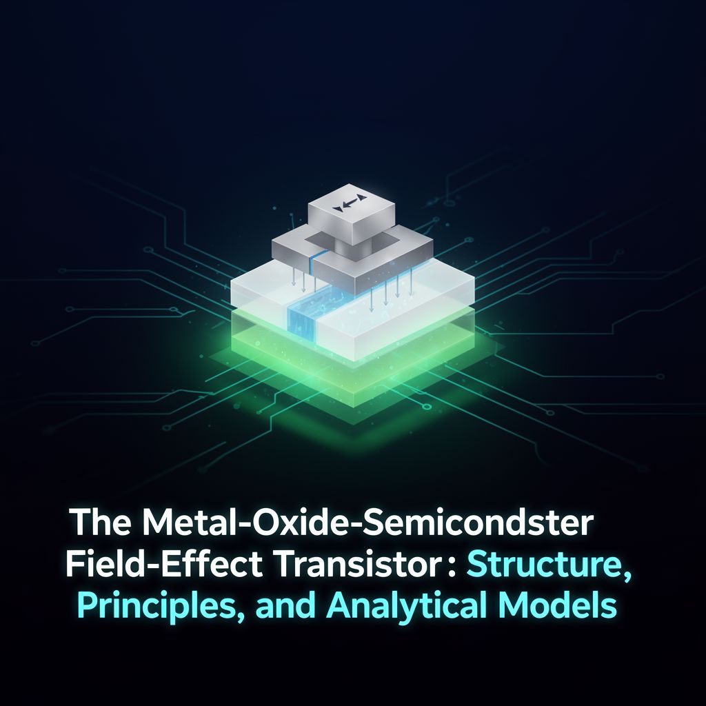
🖼️ Special Focus: Schematic Descriptions of Device Structures
The provided source material refers to figures (e.g., Fig. 40, Fig. 41) that schematically depict various transistor structures. While actual data graphs or plots are not described, understanding these schematic representations is crucial for grasping the evolution of MOSFETs. Below, we elaborate on the visual and structural characteristics of these devices as they would appear in such diagrams.
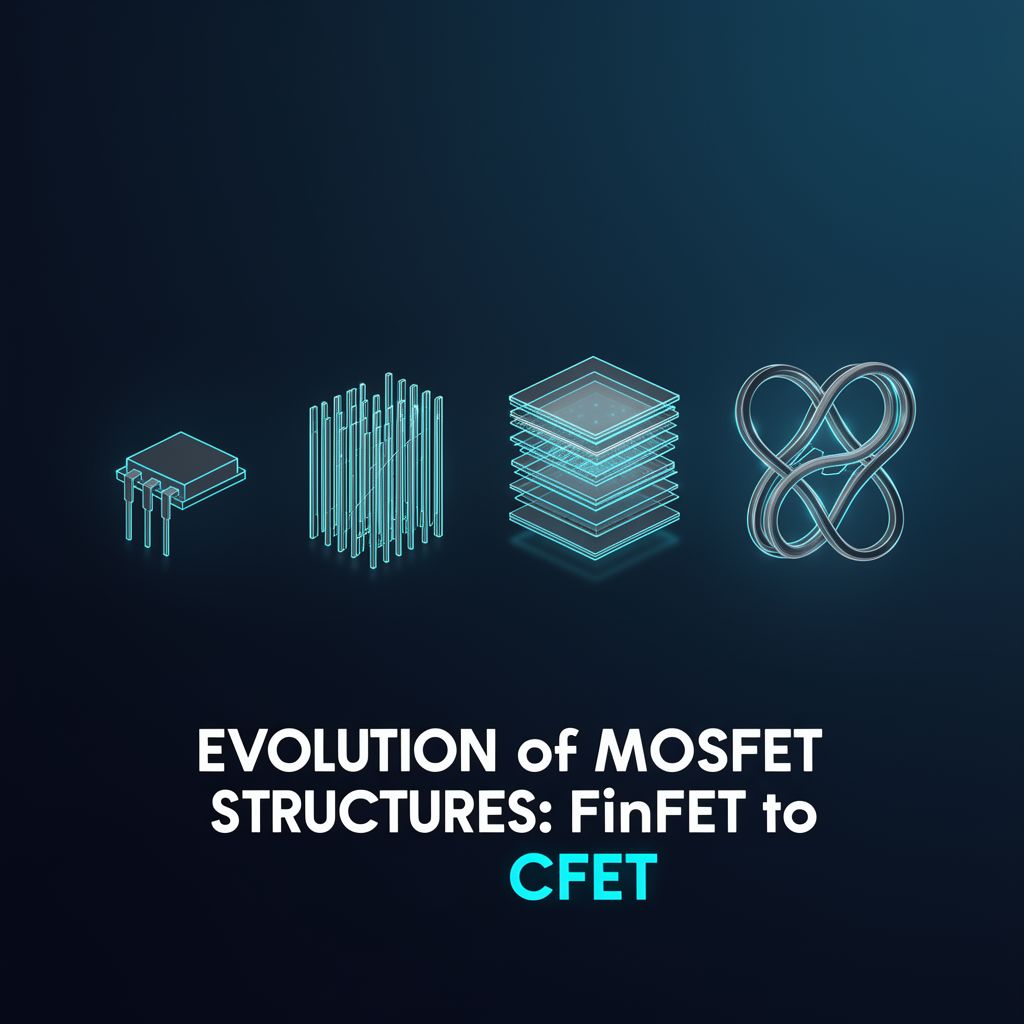
1️⃣ Planar MOSFET (Conceptual Baseline)
- Visual: Imagine a flat, two-dimensional structure on a silicon wafer.
- Key Features:
- A flat channel region on the surface of the silicon substrate.
- A gate electrode positioned directly above the channel, separated by a thin gate oxide (dielectric).
- Source and drain regions diffused into the substrate on either side of the channel.
- Limitation: The gate primarily controls the channel from one side (top), leading to weaker electrostatic control as dimensions shrink.
2️⃣ FinFET (Figure 40(a) - Single-fin, Figure 40(b) - Multi-fin)
- Visual: Instead of a flat channel, picture a thin, vertical "fin" or wall of silicon protruding from the wafer surface.
- Key Features:
- Vertical Fin: The channel is a raised, narrow silicon fin.
- Tri-Gate: The gate electrode wraps around three sides of this fin (top and two sidewalls). This is a significant departure from the planar design.
- Source/Drain: Located at the ends of the fin.
- Multi-fin: For higher current, multiple fins can be connected in parallel, appearing as several parallel vertical walls with a common gate wrapping around them.
- Benefit (Visual Interpretation): The wrapping gate provides much better electrostatic control over the channel, as it influences the channel from multiple directions, effectively "squeezing" it. This is visually represented by the gate material surrounding the fin.
3️⃣ Nano-sheet FET (NSFET) / Gate-All-Around (GAA) (Figure 41)
- Visual: Imagine one or more thin, horizontal sheets of silicon, stacked vertically, completely enclosed by the gate material.
- Key Features:
- Horizontal Sheets: The channel consists of one or more thin, flat layers of silicon, parallel to the wafer surface.
- Gate-All-Around (GAA): The gate completely surrounds each nano-sheet on all four sides (top, bottom, and two sidewalls).
- Stacking: Multiple nano-sheets can be stacked vertically to increase effective width (W) without increasing the footprint on the wafer.
- Benefit (Visual Interpretation): The complete enclosure by the gate provides the ultimate electrostatic control, as the channel is influenced from every direction. This is visually depicted by the gate material forming a "box" around the channel sheets.
4️⃣ Forks-sheet FET (FSFET) (Figure 41)
- Visual: Picture a pair of NSFETs (one n-channel, one p-channel) placed side-by-side, separated by a thin dielectric wall.
- Key Features:
- Side-by-Side Integration: Two distinct NSFET-like structures are positioned very close to each other.
- Dielectric Wall: A thin insulating wall separates the two devices, acting as a reference for self-alignment and preventing electrical shorting between their source/drain regions.
- Shared Gate Concept: While distinct, their proximity and the dielectric wall facilitate tight integration for complementary logic.
- Benefit (Visual Interpretation): This structure visually represents a compact way to integrate complementary transistors horizontally, saving area compared to separate devices.
5️⃣ Complementary FET (CFET) (Figure 41)
- Visual: Imagine an n-channel NSFET stacked directly on top of a p-channel NSFET.
- Key Features:
- Vertical Stacking: The most striking feature is the direct vertical integration of complementary devices.
- Split Nano-sheets: Vertically stacked nano-sheets are divided, with the lower group forming the p-channel device and the upper group forming the n-channel device.
- Independent Source/Drain: Each device has its own independent source and drain regions.
- Benefit (Visual Interpretation): This is the ultimate in area efficiency for complementary logic, as it halves the footprint by stacking devices. Visually, it would appear as a multi-layered sandwich of channel sheets and gate material.
These schematic descriptions highlight the geometric innovations that have driven MOSFET evolution, each designed to enhance gate control and overcome the physical limits of miniaturization.